

What is the Role of Laser Drilling in HDI PCB?
In the rapidly evolving world of electronics, HDI PCBs (High-Density Interconnector PCBs) have become essential for creating compact, high-performance devices. These PCBs enable the miniaturization of electronic products while ensuring efficient signal transmission and high reliability. One of the most critical processes involved in the production of HDI PCBs is laser drilling. Laser drilling plays a significant role in the creation of microvias, which are essential for the complex layer connections in HDI PCBs. In this article, we will explore the role of laser drilling in HDI PCBs and its importance in modern electronic manufacturing.
Understanding Laser Drilling in HDI PCB Manufacturing
Laser drilling is a highly precise method used to create holes in hdi pcb, especially for the creation of microvias. Unlike traditional mechanical drilling, which uses rotating bits to cut through the PCB material, laser drilling utilizes focused laser beams to burn or vaporize material in a controlled manner. This results in extremely fine holes with high precision, making it ideal for drilling microvias, which are smaller than those used in conventional PCBs.
Laser drilling is crucial for HDI PCBs due to the complex nature of these designs. HDI PCBs often contain multiple layers, with intricate routing requirements that need smaller, more precise holes for electrical connections between layers. Laser drilling enables the creation of these small holes with diameters as small as 50 microns, which would be difficult or impossible to achieve with traditional mechanical methods.
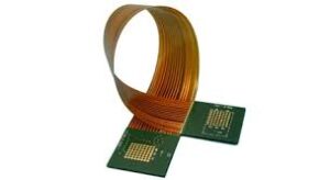
The Advantages of Laser Drilling in HDI PCBs
1. Precision and Accuracy
One of the main reasons laser drilling is so essential in HDI PCB production is its precision. Laser beams can be focused with extreme accuracy, allowing manufacturers to drill very small and perfectly aligned holes in the PCB. This is particularly important in HDI PCBs, where microvias need to be created with high precision to maintain signal integrity and ensure reliable electrical connections between layers.
The ability to drill fine holes with accuracy is critical for high-density interconnects, as it ensures that the vias are properly aligned with the circuitry on both sides of the PCB. This precision reduces the risk of defects such as misalignment, which could compromise the performance of the final product.
2. Miniaturization
HDI PCBs are specifically designed to support the miniaturization of electronic devices. In such designs, space is at a premium, and every component must be placed as efficiently as possible. Laser drilling enables the creation of smaller vias, which is crucial for maintaining a compact PCB layout while still supporting multiple layers of interconnects.
The small size of the vias created by laser drilling also allows for more compact designs, enabling manufacturers to produce thinner and lighter devices. As the demand for smaller, more powerful electronics continues to grow, laser drilling will play an increasingly important role in achieving these goals.
3. Improved Signal Integrity
Signal integrity is a top priority in HDI PCBs, especially in high-speed applications. Microvias created through laser drilling help maintain the quality of signals by providing shorter and more direct electrical paths between layers. This helps reduce resistance and prevents issues such as signal loss, noise, and interference that can occur with larger vias or longer routing paths.
The precision of laser drilling also ensures that the holes are uniformly sized and aligned, which is essential for the consistency of electrical performance across the entire PCB. This contributes to the overall reliability and functionality of the final product.
4. Faster Production and Flexibility
Laser drilling is a faster and more flexible method compared to traditional mechanical drilling. The speed of the laser drilling process allows manufacturers to produce HDI PCBs more quickly, reducing lead times for complex designs. Additionally, laser drilling can be used to create vias of various sizes and shapes, offering greater flexibility in the design and production of HDI PCBs.
This speed and flexibility make laser drilling an ideal choice for high-volume production runs, especially in industries where time-to-market is critical, such as consumer electronics and automotive sectors.
Conclusion
Laser drilling is a vital process in the creation of HDI PCBs, providing the precision, accuracy, and speed needed to produce the small, densely packed vias that are characteristic of these advanced circuit boards. Its role in microvia creation enables the miniaturization of electronic devices, enhances signal integrity, and supports faster production times. As the demand for smaller, more efficient electronic devices continues to rise, laser drilling will remain a key technology in HDI PCB manufacturing, ensuring that the next generation of electronics meets the performance and size requirements of modern applications.