

Connection Between PCB HDI and Miniaturization
PCB HDI, which stands for high density interconnection, is one of the most important innovations in the electronic industry. It allows for more interconnections in smaller areas, making it ideal for electronic devices like smartphones and medical equipment that require compact, lightweight circuit boards. The technology offers many benefits, including enhanced signal integrity and reduced power consumption. In addition, its design procedures allow for more complex electronics with faster and better performance.
The pcb hdi process begins with the careful selection of substrate materials based on specific electrical performance requirements. The layers are then pre-treated to eliminate contaminants and ensure adhesion prior to lamination and drilling. The resulting layer build-up is subjected to high temperatures and pressure, which bonds the materials together into a solid composite structure.
Once the layers are bonded together, they are cut and drilled to create a matrix of fine lines called vias. The fine holes are created using laser drilling techniques and have a much smaller diameter than traditional through-hole vias. This enables the interconnections to be made in a much smaller space, which frees up more room on the surface of the PCB.
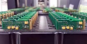
The Connection Between PCB HDI and Miniaturization
To further maximize the space on a board, designers use strategic routing to route signals between layers. They may also group components with similar functions or corresponding signals together, which reduces interference and improves functionality. With proper planning and analysis, this can help to minimize component size while maintaining performance standards.
Another factor affecting performance is the layout. Creating an efficient PCB requires precise placement of components and vias, which is possible with HDI. This enables designers to utilize a smaller footprint and lower the number of layers required, which cuts costs while improving overall quality.
In addition to the advantages mentioned above, HDI PCBs offer excellent reliability. This is due in large part to the fact that microvias have a lower aspect ratio than traditional through-hole vias. This results in a more reliable connection and improved plating stability. The tighter connections and smaller components also result in a reduction of thermal resistance, which enhances the performance of the circuit board.
With the increased complexity of modern devices, the need for higher performance in small form factors has become more critical than ever. This has fueled the rapid expansion of the IoT industry, where small devices are stationed in remote locations and need to be self-sufficient in terms of power. HDI PCBs are a great solution for these applications, offering the space and performance needed to support advanced technologies like 5G wireless communication.
In order to achieve the best results, designers must follow strict guidelines when constructing a PCB with HDI technology. The thickness of the traces and the width of the microvias are just two of the factors that need to be carefully considered. In addition, proper design of the power and ground planes is crucial to ensuring the integrity of the electrical connections. Finally, the use of a copper foil with the appropriate dielectric characteristics is key to maximizing performance.