

Properties of Flex Circuit PCBs
When properly designed and constructed flex circuit PCBs are able to withstand millions of bending cycles over product lifetimes. They can be found in a wide variety of devices including consumer electronics, automotive, medical and aerospace. However, it is critical that the fabricator knows what can cause a flex circuit to fail in the field – factors like heat, moisture, chemicals, shock and vibration – so that they may provide adequate mechanical support to the flexible components.
Specialized materials and construction techniques make flex PCBs the perfect solution for dynamic applications. The most popular flex PCB construction consists of a Polyimide dielectric substrate cladded with ultra-thin rolled copper foils. These foils are patterned using lithographic processes to create the required conductive paths or traces. Copper thickness can range from.0007″ to.0028″. The thinner the copper, the more flexibility the flex circuit has.
Conductors are bonded to the flex substrate with adhesives that offer either thermal or pressure-sensitive bonding. The bonded copper can then be plated with an assortment of surface finishes to protect it from damage. These surface finishes include solderable nickel, tin, gold, silver and various specialty finishes to enhance conductivity, provide corrosion resistance, and meet specific environmental requirements.
To reduce the risk of failure due to stress, flex PCBs often incorporate structural reinforcement at the flex-to-rigid joins or interfaces. These stiffeners can be made of silicones, hot-melt adhesives or epoxy resins and are applied in a pattern that corresponds to the board’s flexing characteristics. In addition to providing physical rigidity, these structural elements help to distribute the load over the entire flex circuit pcb assembly and improve its reliability by eliminating localized points of stress.
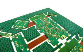
Mechanical Properties of Flex Circuit PCBs
Another important aspect of the flex PCB design is the selection of a suitable etch process for the copper layers in order to ensure proper conductor control and impedance at high speeds. This is where button plating (where copper is deposited only on the pads/vias) can offer significant advantages over panel plating.
A specialized coating can also be added to the flex-to-rigid interfaces to prevent fatigue cracking, stress, and strain on the connection between the rigid board and flex circuit. This is especially useful in harsh environments where environmental stresses can rapidly fatigue and weaken the flex-to-rigid joint.
Careful consideration is needed for aspects like trace spacing, copper thickness, bend radius, vias, adhesives and tear propagation in flex circuits to ensure they can survive the demanding conditions of dynamic applications. Proper modeling with accurate material properties allows the flex-to-rigid connections to be engineered and manufactured to survive the dynamic bending and vibrations that occur in many of today’s most advanced mobile devices, automotive electronics and aerospace and defense systems.
If these flex circuits aren’t built with these considerations in mind, they can quickly fail in the field due to excessive stress, damage and/or premature failure. To avoid these issues, it is important to work with an experienced flex circuit manufacturer that understands the intricacies of the manufacturing process and has the tools to ensure your flex circuits can withstand thousands or even millions of flexing cycles over the lifetime of your device.