

Reliability of High Density Interconnect
High density interconnect (HDI) technology has been a major enabler of advancement in electronics. The technique allows densely packed electronic devices to achieve higher performance with smaller footprints compared to traditional multi-layer PCBs. HDI PCBs are used in state-of-the-art consumer electronics like smartphones, tablets and wearables, IoT products like smart meters and appliances, as well as sophisticated industrial automation equipment for warehouse management and other business applications.
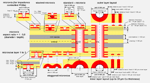
To achieve the superior reliability of high density interconnect PCBs, designers must carefully consider a number of factors. These include component placement, stack-up configuration and thermal/mechanical analysis. Additionally, designers must consider the use of microvias to reduce via hole diameters and improve signal integrity. The use of advanced copper plating and solder masks can also help to increase the reliability of a board.
The use of blind vias in a PCB enables higher signal transmission rates and lower crossing intervals. This leads to a faster data transfer rate, which in turn translates into higher device performance and enhanced functionality. However, implementing these features in a circuit board requires extensive testing to ensure that they are working properly.
How to Test the Reliability of High Density Interconnect
Creating effective HDI circuit boards entails utmost diligence throughout the entire manufacturing process, and then extensive testing to ensure that they are up to industry standards. A comprehensive test flow is essential to ensuring that the integrity and functionality of a circuit board are protected against all possible stressors, including signal loss, current consumption, component tolerances, and more.
In addition to evaluating the performance of each of these components, it is important to evaluate the effectiveness of the PCB in its intended environment. This is especially true for boards that are intended for use in hazardous environments, such as military and aerospace applications. Using a standard test flow such as IPC-TM-650 or one that is tailored to the product’s environment can help ensure that the boards will be able to withstand any environmental stresses that may arise during operation.
While any bare PCB can fail under severe conditions, it is particularly critical to understand the failure modes and stressors that may be encountered in the product’s intended environment. This will allow engineers to test for these specific conditions in order to identify the most likely sources of failure and take steps to prevent them.
The use of microvias in a PCB can significantly increase its reliability, but this requires careful consideration during design. The design of a microvia system should include an optimization of the layout and material selection to ensure that it will perform as required in the end product. A comprehensive test flow is critical to achieving this goal, and it is important to look at the entire product life cycle when developing a test strategy for a new type of PCB. In addition, manufacturers should consider the use of multiple sequential layers to minimize the amount of vias and to avoid overlapping connections. This will minimize the likelihood of a microvia failure due to crosstalk between different layers.