

RF Board for Different Frequencies
RF (radio frequency) boards are vital components in today’s high-speed technology. They support cellular base stations, smart wearables, and more. With high frequencies and sensitive signals, RF boards require careful design and manufacturing. Proper grounding, impedance matching, and careful layout help ensure signal integrity and performance. Testing and prototyping are also critical to ensuring that the final product works as intended.
Using an RF board requires selecting materials with the right properties. The underlying substrate has significant influence on signal integrity, thermal management, impedance uniformity, and dimensional stability. RF PCBs are typically made with FR-4 glass epoxy, although alternatives like PTFE can offer better thermal properties and performance.
Selecting the right etching and soldering processes for rf board is another important factor in achieving optimal performance. These processes are required to withstand higher temperatures than traditional PCBs, and they must have the capability to register align multiple layers during assembly.
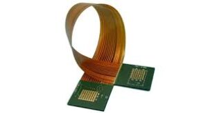
How to Customize an RF Board for Different Frequencies
The choice of RF PCB laminates is also crucial for optimizing performance. RF circuits require thinner laminates than traditional PCBs to avoid unwanted loss and distortion of the RF signal. The dielectric constants of the PCB laminates also play an important role. The ideal RF circuit board uses low-loss laminates with an optimum Dk value to reduce loss.
Another essential consideration is RF circuit board parasitics. These parasitic effects are caused by the interaction of RF signals with other components and features on the board. To minimize parasitics, RF designers must separate analog, digital, and radio signals to reduce interferences between them. They must also pay close attention to trace lengths, and avoid placing unrelated inputs and outputs next to each other.
For example, a plated through via hole (PTV) can introduce inductance into the circuit, which affects signal performance. These effects can become even more noticeable at higher frequencies.
Impedance matching is a critical part of RF design, and it must be used to ensure that signals travel smoothly from one component to the next. If the impedance is mismatched, the signals will reflect back and cause distortion. To avoid this, RF designers use techniques like adding matching circuits or adjusting trace widths to match the impedance.
An RF (Radio Frequency) board is a specialized circuit board designed to handle and process signals in the radio frequency range, typically from 3 kHz to 300 GHz. These boards are crucial components in modern electronics and communications systems, playing a key role in a wide range of applications, including wireless communication, radar systems, satellite communication, and medical equipment. RF boards are designed to facilitate the transmission and reception of high-frequency signals, often involving complex circuit designs and materials to ensure proper performance at these high frequencies.
RF PCBs must also be designed to accommodate varying impedances and capacitances. This is especially true for transmission lines, which must have precise dimensions to maintain controlled impedance. Fortunately, specialized RF software can assist with this process by calculating the proper dimensions for each trace. Proper placement of transmission lines is also essential to reducing losses and maintaining high performance. This includes minimizing interference from adjacent traces, connectors, and antennas. Finally, RF designers must carefully consider the location and orientation of high-frequency components, as they can radiate energy outside of the circuit board.