

Micro Vias Affect the Reliability
A micro via is a smaller version of a traditional through-hole (TH) or blind via in a printed circuit board (PCB). These structures are designed to save space on a circuit board by allowing designers to make connections between layers with shorter pitches. This allows for higher component density and can increase the functionality of the final product. However, using microvias is not without its challenges. One of the biggest issues with them is reliability. The reliability of microvias depends on many factors, such as their physical construction and the materials used. Taking all of these factors into account can help ensure that a PCB with microvias is reliable and will last a long time.
The most common type of micro vias is the stub-end via. This type of via has a conical frustum shape with walls that slope inward toward the center of the hole. This design helps to minimize stress and improve reliability by ensuring that all metal contacts in the via are exposed. It also helps to reduce thermal stresses and the potential for voids in copper plating.
Another type of microvia is the staggered via. Unlike the stub-end via, the walls of a staggered microvia rise up and down in a series of small steps. Staggered microvias are usually used to form interconnections between multiple layers. This helps to reduce the number of layers in a stack and eliminates the need for mechanical soldering or bonding. However, this type of microvia is still prone to failure at the point where stacked microvias meet. This is because the plating thickness of the butt joint at the stack interface can be less than the minimum required for reliable operation.
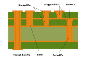
How Micro Vias Affect the Reliability of Vias in Printed Circuit Boards
It is important to note that the reliability of microvias can be significantly impacted by the quality of the copper plating process. Insufficient plating can lead to incomplete copper fill, which can result in voids or dimples in the surface of the microvia. These voids can increase stress levels in the microvia and reduce its fatigue life. In addition, the size and shape of the voids can affect the reliability of the microvia. Small voids with a spherical shape generally have a light effect on the microvia reliability, while extreme void conditions can have a dramatic impact.
When designing a high-density interconnect (HDI) PCB with microvias, it is essential to understand the requirements and specifications of the fabrication process. This includes proper PCB layout, careful selection of laminates and materials, and the use of appropriate tools to minimize manufacturing defects. It is also vital to use a quality inspection process to verify that all the components and traces on the circuit board are properly placed and connected.
In addition, a thorough risk analysis is necessary to ensure that the microvias in the HDI PCB will be reliable. This can be done by comparing the proposed stackup to existing design rules and by contacting your fabricator for their input on manufacturability.